Description
Chip-8 describes an “assembly-like” language and a typically interpreted virtual machine. I built a hardware CPU capable of executing CHIP-8 instructions. This was quite challenging because I built everything as I went instead of planning it all perfectly from the start, and some instructions are much more complex than others. The tutorials by Ben Eater inspired me to build this CPU. Instead of following them step by step, I built many components myself and consulted his videos when I was unsure how to solve something. Because of this “build as I go” mindset (partly because I did not understand everything in the beginning), the modules are not documented in detail, which I really regret.
Very Useful Resources for Chip 8
- My go-to reference for the instruction set http://devernay.free.fr/hacks/chip8/C8TECH10.HTM
- Awesome assembler, simulator,… https://johnearnest.github.io/Octo/
- Very clear tutorials for building a Breadboard CPU https://www.youtube.com/c/BenEater/videos
Caveats
- Because the whole build is based on breadboards the contacts are degrading with time — 3 years after I built it, it is still working, but sometimes glitches happen which is quite unfortunate.
- Chip-8 has some instructions that are not well-defined. I settled on using the standard settings of the Octo project.
- I mostly built it with components I had on hand or that were easily available — therefore some choices were made because of availability and not because of simplicity or elegance.
- Because of limited space and money I sometimes combined parts of the CPU which should not be combined. For example, I used a single SRAM chip to store REG A-F (which itself is quite ugly already) as well as the 16 address deep stack.
- Looking at it a few years later, I can see many questionable design choices, which were mostly due to poor planning. Still, it was an awesome learning experience, and I still love looking at the mess of cables, breadboards, and chips that somehow work in harmony (more or less).
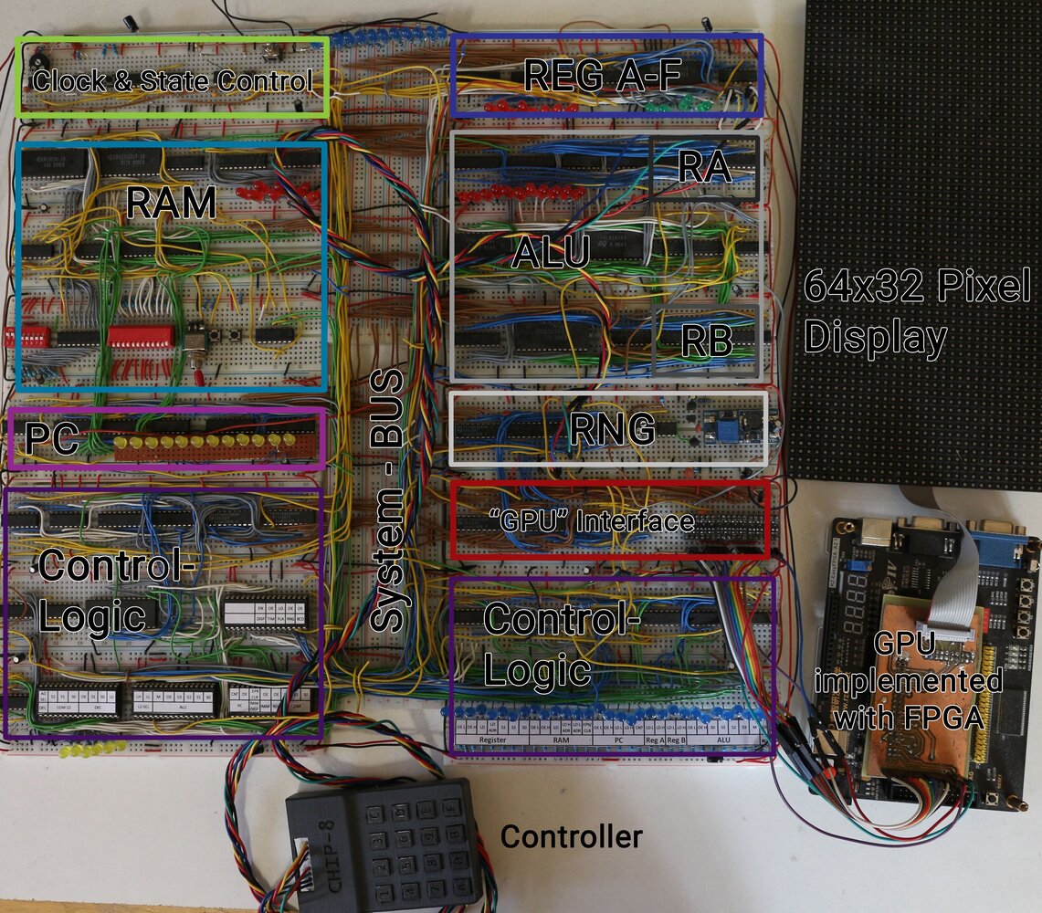
Modules
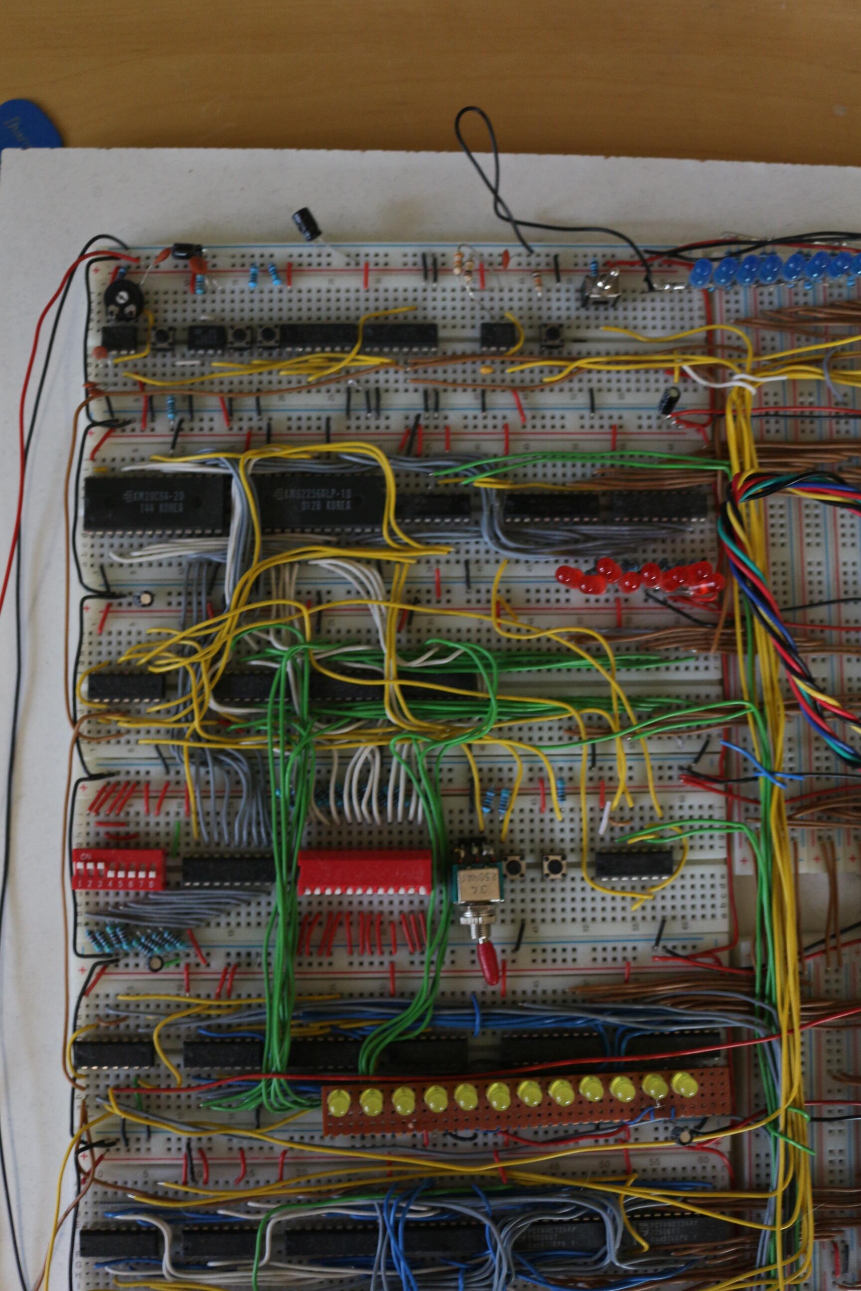
Clock & State Control
This is probably the easiest module and is very similar to Ben Eater’s version. It has an adjustable clock (astable 555, around 100 Hz to 20 kHz), plus start and stop circuits. For development, it also features a single-step mode that uses a monostable 555 to generate pulses. A double-throw switch is used for program loading mode (explained in the RAM module). The last button is a reset button that resets the PC and the microstep counter (inside the control logic).
Program Counter
The job of the program counter is to track where we currently are in the program. It mainly consists of three 74HC193 counters, which can count up and down (only up is used here). The output address is directly connected to RAM (which can take addresses from either the PC or the bus depending on a control flag). The PC can also connect to the normal system bus to load and output its value.
System-bus
Every data word is transmitted over the main system bus in the middle, except for program counter addresses (mentioned above). Each module is connected to the bus using 74HCT244 or 74HC245 tri-state bus drivers. This single bus is probably the biggest bottleneck, but it made interconnecting components very simple, so it fit my “build as I go” style well. My biggest regret is making it 12 bits wide. Early in the project I thought this would be useful because the CHIP-8 address space is 12-bit wide, but in the end I needed all 12 bits for only two or three instructions.
RAM
The main building block of RAM is a KM62256 32Kx8-bit SRAM. RAM also includes a KM28C64 EEPROM for loading programs into memory. Program loading is done by switching Clock & State Control and letting the CPU run briefly (less than half a second), while EEPROM contents are copied into RAM on each clock cycle.
The rest of the circuit (which mostly consists of 74HC157 Multiplexers) is used to manually program the memory which was used during development.
Registers A-F, Stack, Stack-pointer and Register I
Registers are the place where the CPU stores values to operate with. Normally, the registers are a lot faster than the RAM - but in my case this module also uses a single KM62256 (instead of single register chips for space reasons) to store the contents of registers A-F. The registers are told to load from, or output to the bus, by the control logic using three control signals.
The stack as well as register I (a 12-bit index register used for storing addresses) also reside inside the same SRAM chip (not a pretty design choice, but it worked). The stack pointer is implemented directly in hardware using a settable 74HC193 counter. Implementing it as a counter allows slightly faster execution of RET and CALL instructions.
A 74HC157 multiplexer controls whether stack addresses or register addresses are routed to the SRAM module.
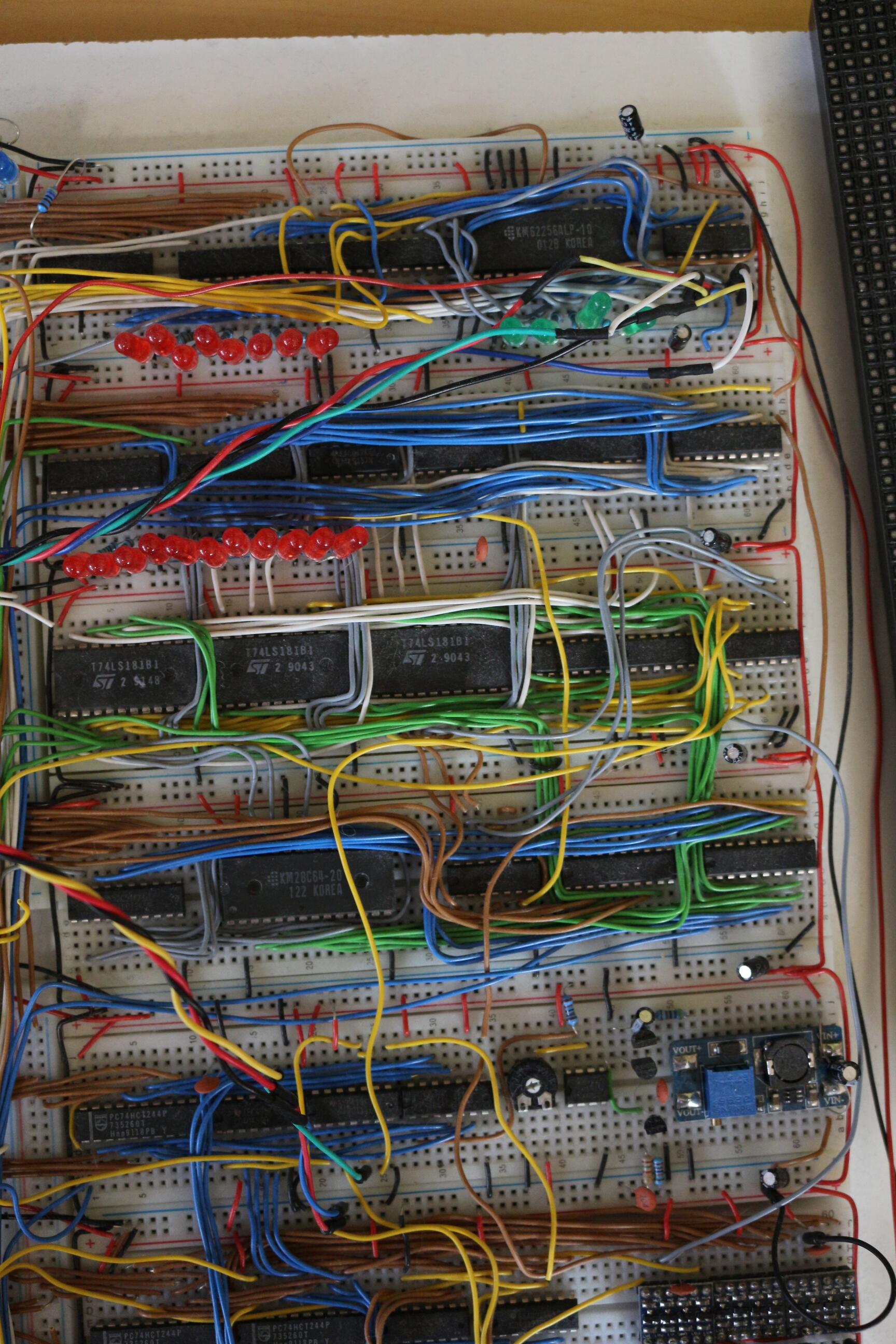
Arithmetic and Logic Unit
The 12-bit-ALU (12 bits for the same reasons as mentioned in the System-BUS part) uses the very useful 74LS181 chips for doing arithmetic and logical operators. It is accompanied by four 74HC377 to load and store the operands from the bus. Another 28C64 EEPROM is used as a “single operand ALU” to implement “esoteric” instructions such as LD B,Vx - “Store BCD representation of Vx in memory”. Simply using an EEPROM as combinatorial logic was the easiest and space-saving solution in this case I think.
Random Number Generator
This CPU actually uses a hardware random number generator. A simple LFSR would probably have been sufficient, but I decided to build a white-noise generator sampled by a shift register. This analog circuit works well, but it is quite sensitive to the potentiometer setting that defines the decision threshold (whether a voltage is interpreted as 0 or 1). In hindsight, I would choose an LFSR.
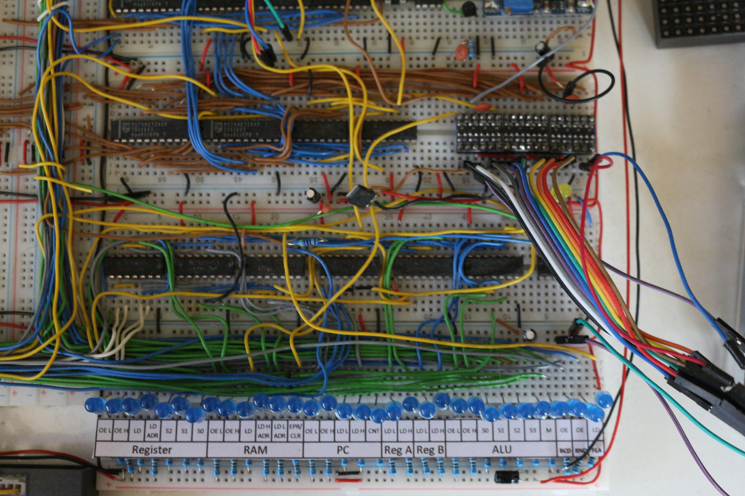
Control Logic
This was probably the most complex part to develop because CHIP-8 instructions are formatted in a fairly impractical way. Each instruction always consists of two bytes. The first 4 bits indicate the instruction type, while the following 12 bits are reused in many different ways. For example, if an instruction is written as Txyn (with each letter representing 4 bits), the n part sometimes encodes data and sometimes specifies a sub-type of instruction. 8xy0 stores register y into register x, while 8xy1 performs a bitwise OR between those registers. Another data-oriented example is 4xkk, which skips the next instruction if Vx != kk. CHIP-8 also uses several addressing modes (immediate, direct, and index), which further complicates decoding.
These issues were solved using a few multiplexers and generic logic gates. The result of this pre-decoding, a 6-bit code corresponding to each instruction, is fed into four parallel flash memory chips SST39SF02 that store the CPU microcode. The whole CPU uses 31 control signals driven by 21 (partly combined) output bits from these memory chips. To track microcode execution state, we need something like a program counter. A 74HC393 counter is used to track the microcode position.
Because of some hard-to-implement instructions, this counter was designed to count up to 63. The longest instructions, Fx65 (read registers V0 through Vx from memory starting at location I) and Fx55, use a whopping 46 microsteps. That is not typical at all; most instructions use around 7 microsteps (including 2 fetch steps). The next section shows what this microcode looks like in my CPU.
Microcode
Microcode is used by the control logic to tell each module what to do, step by step. Let us look at an example instruction, 8xy4 (add registers x and y).
Like most CPUs, this one follows a fetch-decode-execute cycle. The steps required for this addition instruction are:
- Load first Instruction Byte
- Load second Instruction Byte - now the instruction is fully loaded and can be decoded
- Load Register x into ALU Register A (via system-bus)
- Load Register y into ALU Register B (via system-bus) - The ALU is told to add A and B by some control signals
- Output the result to the BUS and store back into register x
- Store overflow-value in VF (this is an example which shows why having all registers in SRAM was a questionable Idea)
- Done (start from step 1 and load next instruction)
Creating Microcode
To create the microcode, I wrote a small Java application that transforms a basic action notation into memory maps for each of the four flash chips. It does not validate whether two actions conflict; it simply sets the corresponding bits for each address.
The actual microcode for the instruction described in Microcode looks like this:
//Vx + Vy , VF= Carry
x x 0: RAM	OEL	DEC	LDH	RB	LDL	PC	CNT //RAM outputs to BUS, Decoder High Register Loads, Program Counter is Incremented
x x 1: RAM	OEL	DEC	LDL	PC	CNT //RAM outputs to BUS, Decoder High Register Loads, Program Counter is Incremented
34 x 2: DEC	Rx  REG	OEL	RA	LDL //DEC Rx lets the Control Logic select Register x, REG OEL tells the Registers to Output its content to the BUS, RA LDL tells the ALU Register A to Load (the lower byte)
34 x 3: DEC	Ry  REG	OEL	RB	LDL	ALU	SUM //Same as above except Register y is selected
34 x 4: DEC	Rx  REG	LDL	ALU	OEL	ALU	SUM	FLA	LD //Register x loads from BUS, ALU outputs to BUS, FLAG bit is loaded
34 0 5: DEC	RF  REG	LDL	BCD	ONE	BCD	OE //If Flag was zero - RF is loading Value from Bus, BCD outputs one, BCD outputs one to BUS (BCD is the special EEPROM unit in the ALU)
34 1 5:	DEC	RF  REG	LDL	BCD	ZERO	BCD	OE //If Flag was one - RF is loading Value from Bus, BCD outputs one, BCD outputs zero to BUS
34 x 6: DEC	RES //Control Logic Resets
The numbers in the front indicate:
- Predecoded value for the instruction
- State of Flag (x-Don’t care,0 or 1)
- Micro-instruction step count
All values containing x mean that any value in this bit must decode to the given control signals. That means one instruction must be written to more than one address in memory (which is once again used as ROM combinatorial logic).
For example x x 0: ... corresponds to 64*2=128 addresses. The 64 comes from 2^6 possible decoded instructions, the 2 from the possible flag - states.
Everything that follows these numbers are Mnemonics which describe what the control signals should do.
Every pair stands for a specific signal: e.g. RAM OEL means: module RAM - output to lower byte of bus. Many other examples can be seen in the code above.
Graphics Card
As mentioned above the GPU is implemented in an FPGA which handles the LED matrix as well as the communication with the CPU. Because the hardware required to drive the led matrix and interpret the CPU signals would be quite huge, I decided to use an FPGA instead of discrete components. Because I set out to build a CPU on a breadboard and not the entire system I think this is a good solution.
CPU side
There is only one instruction which allows writing to the display Dxyn - “Display n-byte sprite starting at memory location I at (Vx, Vy), set VF = collision.”
This instruction takes 26 steps because it needs to push up to 15 bytes to the GPU. The basic protocol in which CPU and GPU communicate looks like this:
- (0-15) amount of Bytes to render to the display,
- x-position
- y-position
- Up to 15 bytes containing the displayed data
- If a bit changes from one to zero in GPU memory (because bytes are written using XOR), the GPU detects this and raises a signal. That signal is received by the CPU and a flag is set.
CPU Microcode for drawing to the display
D x 2: PC	OEHL	RA	LD
D x 3: PC	LDL	REG	OEL	COM	REGIL	DEC	RF
D x 4: PC	LDH	REG	OEH	COM	REGIH	DEC	RF
D x 5: DEC	OE	DISP	LD
D x 6: REG	OEL	DISP	LD	DEC	Rx
D x 7: REG	OEL	DISP	LD	DEC	Ry
D x 8: RAM	OEL	DISP	LD	PC	CNT
D x 9: RAM	OEL	DISP	LD	PC	CNT
D x 10: RAM	OEL	DISP	LD	PC	CNT
D x 11: RAM	OEL	DISP	LD	PC	CNT
D x 12: RAM	OEL	DISP	LD	PC	CNT
D x 13: RAM	OEL	DISP	LD	PC	CNT
D x 14: RAM	OEL	DISP	LD	PC	CNT
D x 15: RAM	OEL	DISP	LD	PC	CNT
D x 16: RAM	OEL	DISP	LD	PC	CNT
D x 17: RAM	OEL	DISP	LD	PC	CNT
D x 18: RAM	OEL	DISP	LD	PC	CNT
D x 19: RAM	OEL	DISP	LD	PC	CNT
D x 20: RAM	OEL	DISP	LD	PC	CNT
D x 21: RAM	OEL	DISP	LD	PC	CNT	ALU	DISP
D x 22: RAM	OEL	DISP	LD	PC	CNT	ALU	DISP	FLA	LD
D x 23: ALU	DISP
D 0 24:	REG	LDL	DEC	RF	BCD	ZERO	BCD	OE
D 1 24: REG	LDL	DEC	RF	BCD	ONE	BCD	OE
D x 25: ALU	OEHL	ALU	A	PC	LD
D x 26: DEC	RES
GPU side
The GPU is implemented in VHDL and runs inside an FPGA. Its job is to translate the protocol from above and set bits in memory accordingly. The memory contents are continuously drawn to the LED-matrix display. This is quite a demanding task because the LED’s need to be PWM controlled as well as multiplexed. Heart of the operation inside the FPGA is a dual-port RAM which allows reading and writing simultaneously at two ports. This is very useful because the CPU side and the LED-matrix side can be separated completely. One port can be used by the CPU side — which is comparably very slow. The other port can be used by the logic to drive the matrix. Controlling the process of multiplexing and PWM is handled by a Finite-state machine.
Results
I was able to run games such as Tetris, Pong, and some great games from the Octojam. Overall, I am very happy with the result and think the project was an awesome learning experience. If I built a second iteration, there are many things I would approach differently, and some things I would keep. The total component cost was around 300 EUR, which is not too bad in my opinion.